The internal registers of the ATmega328P microcontroller
published: 14 December 2020 / updated 14 December 2020

The ATmega328 processor
It is an 8-bit processor with RISC architecture:
- High speed CMOS technology: speed + low consumption
- RISC and Harvard architecture: power in Mips = clock frequency
- power supply between 1.8 and 5.5V
- 3 independent memories:
- built-in flash memory (10,000 write cycles)
- EEPROM memory for semi-permanent data storage (100,000 write cycles)
- fast SRAM memory
Here is the internal architecture of the ATmega328 processor:
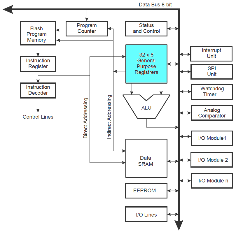
General purpose registers
Here, in blue, the registers of general use. They are 32 in number. are 8-bit registers, listed R0 through R31 .
Some can be used in 16 bits (for indirect addressing):
- X register: R26 (X low byte) R27 (X high byte)
- Y register: R28 (Y low byte) R29 (Y high byte)
- Z register: R30 (Z low byte) R31 (Z high byte)
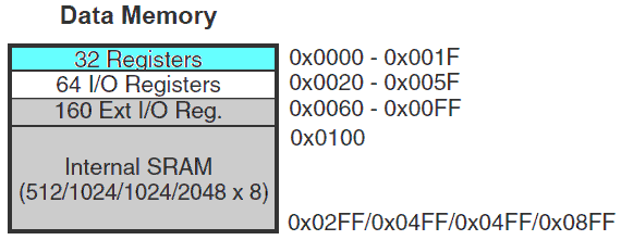
All registers are accessible in the SRAM memory space. For FlashForth, these are addresses between 0000 and 0031 ($ 0000 $ 001f).
To see the content of these registers:
: .num ( c --)
    base c@ >r hex
        0 <# # # #> type
    r> base !
  ;
: regs ( --)
    31 for
        r@ cr dup 3 u.r c@ .num
    next
  ;
It is more than recommended to write directly to these registers.
FlashForth register usage and memory usage
FlashForth uses some of these registers:
- Y(R28, R29): The parameter stack pointer
- X(R26, R27), Z(R30, R31): Temporary data and pointers
- R24, R25: Cached TOS value
- R22, R23: Internal flags
- R20, R21: The P register
- R18, R19: The A register
- R0, R1, R16, R17: Temporary data for assembler words.
- R4, R12, R13: CPU load measurement result (optional).
- R14, R15: Millisecond counter.
- R10, R11: Buffered flash page address.
The A and P registers are FlashForth specific registers.
Register A
This register can be used as temporary storage of data, a reference address for example. To manage several processing loops on a memory area, it can be more interesting to relieve the data stack by putting this address in this register A.
To store a value in the A register:
$00ff >a
hex
a> a> . . \ display ff ff
Executions of > a do not have to be balanced with a>
The contents of the A register are not persistent after the execution of a word.
P register
This register is accompanied by a number of definitions allowing it to be used optimally:
- !p ( addr -- )
Store addr to p(ointer) register - @p ( -- addr )
Fetch the p register to the stack - p+ ( -- )
Increment P register by one - p2+ ( -- )
Add 2 to P register - p++ ( n -- )
Add n to the p register - p! ( x -- )
Store x to the location pointed by the p register - p@ ( -- x )
Fetch the cell pointed by the p register - pc! ( c -- )
Store c to the location pointed by the p register - pc@ ( -- c )
Fetch the char pointed by the p register
Example:
: myStr ( --- addr len)
    s" FORTH is a powerfull language" ;
: toUpType ( addr len ---)
    swap !p
    for
        pc@
        dup  [char] a  [char] z  within
        if
            32 -
        then
        emit
        p+
    next
  ;
myStr type      \ display: FORTH is a powerfull language
myStr toUpType  \ display: FORTH IS A POWERFULL LANGUAGE
Good programming
Marc PETREMANN